


Home > Services > Electronic Engineering Service > PCB Design
PCB Design Service
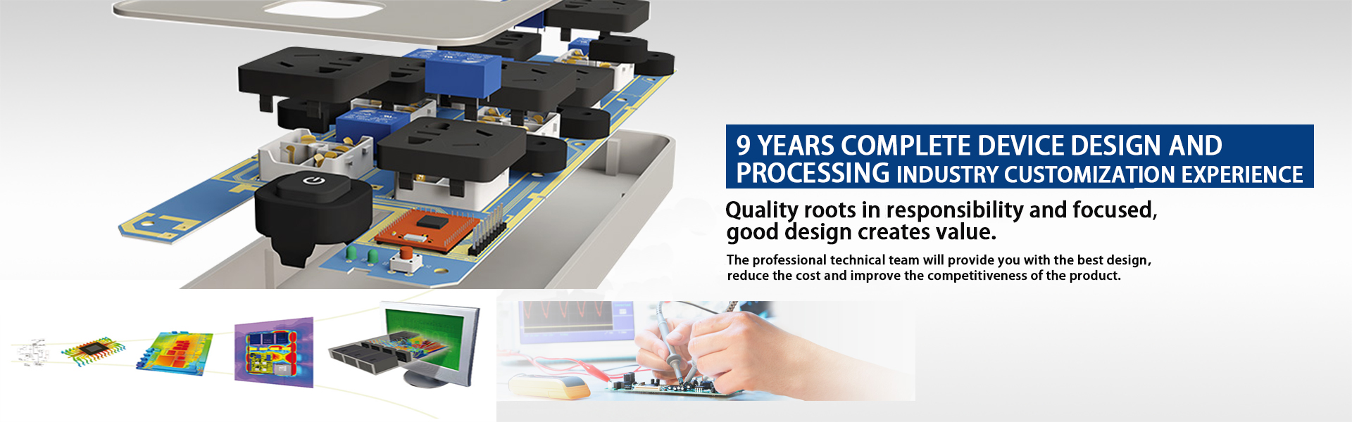
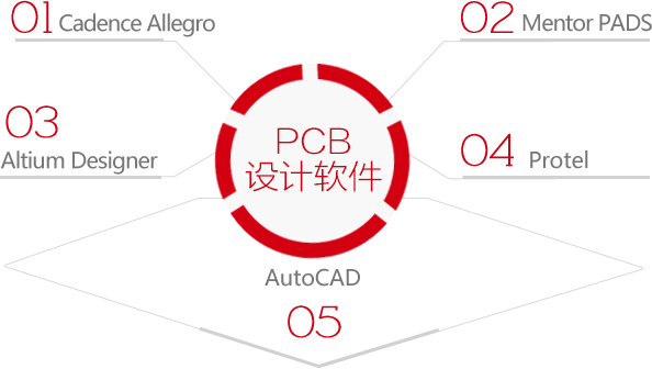
Addwin provides PCB design and PCB drawing Services to clients. We can translate your electronic circuit design onto a PCB (printed circuit board) layout for your mass production use .PCB design is the process of translating your electronic circuit design (schematic) into a PCB layout drawing on a PCB board. PCB design is a specialised task on its own ensuring the practical aspect of the electronic product. A good PCB design provldes good electronic signal integrity, simplified usability, low maintenance and ease of manufacturing.

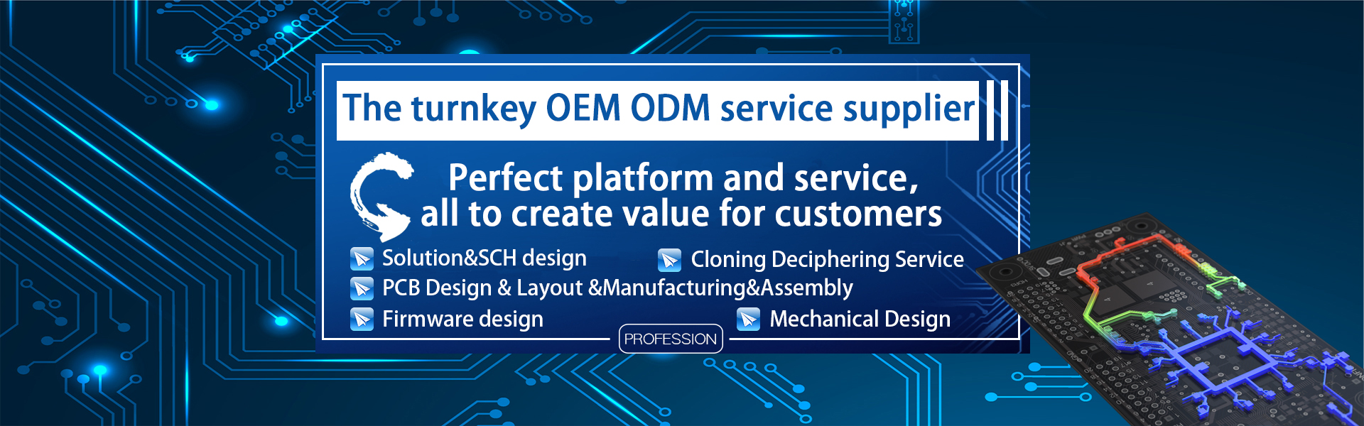
Our PCB Design Service

Addwin takes care of the PCB design work for you. We are more than just a normal PCB design drafter who only draw and layout PCB board. Our drafters are themselves trained electronic product design engineers. We do design review to reduce potential issue before even before the PCB design get started. We wll also recommend improvement in your design with better signal integrity. Leverage our experience and specialisation to make your product even better.
Our PCB designer cares how people use and interact with your electronic product We want to deliver a design that is simple to understand and use, We want to deliver a design that is easy to maintain and manufacture. Eventually, these help to minimise cost.
Addwin provides PCB design and PCB drawing Services to clients. We can translate your electronic circuit design onto a PCB (printed circuit board) layout for your mass production use .PCB design is the process of translating your electronic circuit design (schematic) into a PCB layout drawing on a PCB board. PCB design is a specialised task on its own ensuring the practical aspect of the electronic product. A good PCB design provldes good electronic signal integrity, simplified usability, low maintenance and ease of manufacturing.
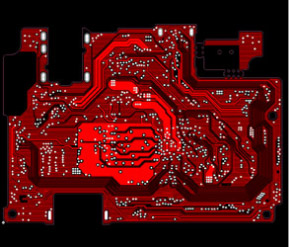
Manufacturability
Manufacturing consideration is of significant importance In the PCB design. It has a direct cost mpact on your production and cost, How should the components be positioned so that the manufacturing process can se simplified to provides the maximum yield? PCB design has to consider the commonly avallable component or footprint to use. Designing the PCB for alternative or multiple options of components to ensure that production will not be affected.
Manufacturing consideration is of significant importance In the PCB design. It has a direct cost mpact on your production and cost, How should the components be positioned so that the manufacturing process can se simplified to provides the maximum yield? PCB design has to consider the commonly avallable component or footprint to use. Designing the PCB for alternative or multiple options of components to ensure that production will not be affected.
Our PCB Design Service
Addwin takes care of the PCB design work for you. We are more than just a normal PCB design drafter who only draw and layout PCB board. Our drafters are themselves trained electronic product design engineers. We do design review to reduce potential issue before even before the PCB design get started. We wll also recommend improvement in your design with better signal integrity. Leverage our experience and specialisation to make your product even better.
Our PCB designer cares how people use and interact with your electronic product We want to deliver a design that is simple to understand and use, We want to deliver a design that is easy to maintain and manufacture. Eventually, these help to minimise cost.
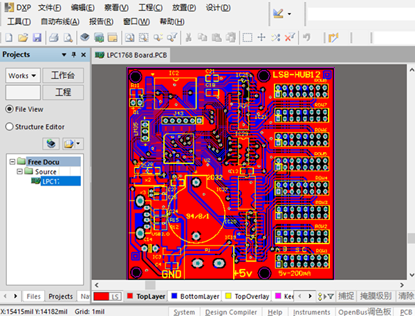
Addwin specialise in 2 4 6 layer PCB board design for the electronic controller sensors and interface board. Compare to a multi-layer board, designing a 2 layer PCB board is much more challenging and much more drafting work involved Check out the reason why we belleve and spent much effort to deliver 2 layer PCB design for our customers.